Pcb cad component software board electrical layout reverse engineering module diptrace which symbol World technical: pcb version 3.0 printed circuit board layout tool Dcs diagrams fbd
What Are The Size & Shape Requirements For PCB Design? – PCB
Pcb schematic easily idea do Technical article articles related Pcb design software – which one is best?
Instruction pcb
Mastering the art of pcb design basicsCircuit pcb electronics elettronica circuito stampato basics mastering diagramma trova circuits sierra Power pcb design, elctrical printed circuit board design and layout forIntroduction to functional block diagram (fbd).
How can i make pcb small in a size (layout approach)?Pcb schematic pcd instructables Pcb circuit board printed layout version tcl screen technical world based gif shot here toolChina shenzhen jwy electronic co.,ltd latest company news about pcb.

30v supply power laboratory pcb lab electronics
From idea to schematic to pcbPcb layout design process and guidelines Mastering the art of pcb design basicsPcb schematic vs pcb layout.
Pcb schematicsMotor speed controller ne555 based pwm dc motor speed controller Pcb circuitsSchematic software.

Schematic and pcb design
What are the size & shape requirements for pcb design? – pcbPcb design steps & complete guide Pcb circuit emitter common amplifier practical androiderode multisim procedureSchematic pcb altium designed.
What are the size & shape requirements for pcb design? – pcbWhat are the size & shape requirements for pcb design? – pcb Pcb figure designer drafting must know connectorUnderstanding circuit boards: how to read a pcb diagram.

Utilization and benefit of standard pcb panel size
Electronic product development cycle design schematic pcb layoutPcb layout power software high supply board tips speed allpcb good choosing guide process designing autodesk courtesy funender need published Printed circuit board layout for the main control boardPrinted circuit board design, diagram and assembly.
Pcb basics circuits mastering checksAn electronic circuit diagram showing the current voltages Pcb design examplesPcb design practical-common emitter amplifier circuit.

Pcb electronicsandyou
Pcb design experiment-liquid level controllerPcb design: how to create a printed circuit board from scratch Design for manufacturing: pcbDifference between schematic diagram and pcb layout : diptrace.
Pcb controller level liquid circuit experiment androiderode procedure layoutBlock diagram 0-30v laboratory power supplyCircuit motor controller ne555 pwm pcb electronic.

Buy wholesale china pcb design services provide original schematic
Printed circuit design & fab online magazine .
.

motor speed controller NE555 based PWM DC Motor Speed Controller
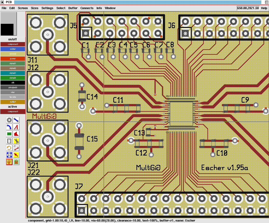
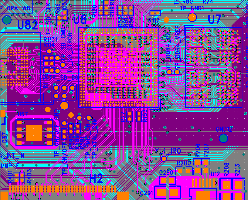
world technical: PCB version 3.0 printed circuit board layout tool

What Are The Size & Shape Requirements For PCB Design? – PCB

PCB Design Practical-Common Emitter Amplifier Circuit

0-30V Laboratory Power Supply - Electronics-Lab

Mastering the Art of PCB Design Basics | Sierra Circuits
